Computational Condensed Matter and Nanoelectronics
The CCMN research performs state-of-the-art ab initio computational modelling that discerns the underlying quantum mechanical nature of organic and crystalline materials as well as heterostructures, from the point of view of fundamental physics and technological applications in nanoelectronics and optoelectronics.
Research
At CCMN, our research efforts focus on the following scientific areas that span across condensed matter physics, solid state physics, materials science and nanoelectronics. We are always looking for new research collaborations, so please get in touch if you are interested in working with us.
Electronic structure of materials surfaces and interfaces
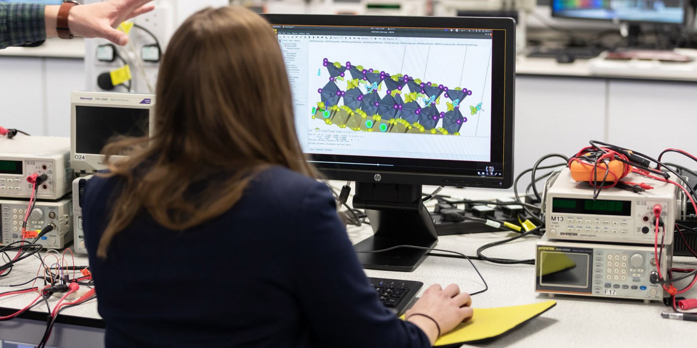
In electronic and optoelectronic devices, such as field-effect transistors, solar cells and light emitting diodes, it is crucial to optimise the energy level alignment between materials interfaces, in order to improve device efficiency. We work in close contact with experimental groups that are experts in device fabrication and use our computational methodology complementary to acquire deeper understanding of the interplay between materials interface science and device physics in the presence of defects and impurities. We use a combination of density functional theory and Poisson equation to quantify charge transfer between thin film layers in the device. Such layers can be either conducting or semiconducting. Upon the creation of the interface, we investigate i) the appearance of gap states in the n- or p-type semiconductor, ii) the occurrence of Fermi-level pinning, iii) the work function modification of the metal substrate due to the formation of the metal/semiconductor interface, and iv) the consequent effect on energy level alignment at the very interface. Agreement is sought between theory and experiment via UPS and XPS measurements. Our computational methodology provides insight into how the work function of the anode and cathode could be tuned to provide efficient electron injection/collection and finally be transformed into high‐performance optoelectronic device electrodes. Selected publications in this area are as follows:
- Y. Zhou et al. Science 336, 327 (2012).
- T. A. Papadopoulos et al. Adv. Funct. Mater. 23, 6091 (2013).
- E. Polydorou et al. Nano Energy 34, 500 (2017).
- M.-K. Lin, et al. Phys. Rev. B 95, 085425 (2017).
Please contact Dr Theodoros Papadopoulos for further information.
Charge and exciton transport in organic thin films
Our work is related to applications such as Organic Photovoltaics (OPVs), Organic Light Emitting Diodes (OLEDs), and Organic Field-Effect Transistors (OFETs). The theoretical methodology we use is based on the combination of Molecular Dynamics to predict the morphology of organic thin films and Kinetic Monte Carlo modelling, parametrised via ab initio methods, to simulate electron, hole, or exciton transport. We carry out a systematic comparison with available experimental data, and analyse the role that the dynamic nature of positional and energetic disorder play on the temperature and electric field dependence of charge mobility, or exciton diffusion length. Our work establishes a clear link between microscopic and macroscopic transport quantities and utilises nanoscale theoretical schemes as a tool for predictive material screening towards efficient organic optoelectronic applications. Selected publications in this area are as follows:
- T. A. Papadopoulos et al. Chem. Sci. 2, 1025 (2011).
- S. M. Gali et al. J. Chem. Phys. 147, 134904 (2017).
Please contact Dr Theodoros Papadopoulos for further information.
Molecular electronics
Using a first-principles approach that combine density functional theory, scattering theory and Green functions within the Landauer-Buttiker formalism, we study the electron transport properties of molecular wires, which may form the interconnects for future molecular electronics devices. Conductance and IV curves are extracted to characterise a wide range of molecular nanodevices. Via our methodology, the occurrence of Breit-Wigner and Fano resonances are explored to identify whether electron transport can be controlled via imposing conformational modifications on the molecular wire itself, acting hence as a molecular diode or sensor. Selected publications in this area are as follows:
- T. A. Papadopoulos et al. Phys. Rev. B 74, 193306 (2006).
Please contact Dr Theodoros Papadopoulos for further information.
Quantum Monte Carlo Modelling
We are also engaged in fundamental computational research exploring the electron-electron interaction, in the homogeneous electron gas (HEG), employing the quantum Monte Carlo technique. The HEG consists of a sea of electrons together with a uniform positive background charge density. Information gleaned from numerical studies of the HEG form the basis of the exchange-correlation functionals, used in almost all density functional theory simulations of real materials. We also investigate the Coulomb attraction between electrons and holes in layered semiconductor systems. Our calculations show that at low electron densities isolated few-body species are present, while at higher electron densities collective, many-body behaviour is observed. Selected publications in this area are as follows:
- G. G. Spink et al. Phys. Rev. B 88, 085121 (2013).
- G. G. Spink et al. Phys. Rev. B 94, 041410(R) (2016).
Please contact Dr Graham Spink for further information.
Quantum Dot Cellular Automata
QCA devices and circuits are a brand-new paradigm for computer architecture. QCA are transistorless and the charge configuration of quantum dots encodes binary information. In particular, we perform numerical calculations for the switching of QCA mixed valence molecule and simulate the Clocking of Molecular QCA, by lithographically defined wires, buried in the substrate, with the molecules located at the surface. Selected publications in this area are as follows:
- M. Alharbi et al. Nanomaterials 13, 2445 (2023)
- M. Alharbi et al. J. Supercomput. 79, 11530 (2023)
Please contact Dr Richard Stoker and Dr Gerard Edwards for further information.
Dr Theodoros Papadopoulos
Associate Professor
Dr Graham Spink
Senior Lecturer
Dr Richard Stocker
Senior Lecturer
Students
MRes and PhD students who would like to work with us are advised to first identify a CCMN area of research interesting to them and then contact our research academics to discuss the possibility of formulating a research project of their interest. Submitting research proposals with motivated students is always within our interest, so please do get in touch!
PhD and MRes students in the CCMN group are as follows.

Visiting PhD researcher: From Dec. 2024, postdoc at the Institute for Solid State Physics, University of Tokyo.
I am a PhD candidate, from the Department of Physics and Center for Theoretical Physics, National Taiwan University (NTU). My PhD studentship is funded by the Taiwan International Graduate Program in Nanoscience and Technology, Academia Sinica, Taipei, Taiwan (R.O.C.). As a visiting PhD student at the University of Chester (UOC), I work under the supervision of Dr Theodoros Papadopoulos and Prof Guang-Yu Guo, National Taiwan University, as part of a Royal Society and Ministry of Science and Technology (MOST), grant awarded to UOC and NTU respectively.
My research primarily focusses on first-principles electronic structure modelling of materials surfaces and interfaces, with applications in optoelectronic devices such as perovskite solar cells (PSCs). Specifically, I look into charge transfer at device interfaces such as between the electron transport layer and perovskite layer. Our task is threefold; we aim to (i) reduce PSCs toxicity by using Pb-free perovskites, (ii) acquire better understanding of the nanoscale variables that influence the energy level alignment at the device interfaces, and (iii) improve device performance by choosing an appropriate combination of materials that reduce device interface energy barriers, hence improving photo conversion efficiency.
My research efforts at NTU under the supervision of Prof Guang-Yu Guo, are towards the study of quaternary arsenide compounds XCuYAs (X=Zr,Hf; Y=Si,Ge) that are part of a family of materials that possesses outstanding physical properties ranging from p-type transparent semiconductors to high-temperature Fe-based superconductors. I study the electronic structure topology, the spin Hall effect (SHE), and the spin Nernst effect (SNE) in these compounds based on density functional theory calculations. My work in this area is published in Phys. Rev. Materials 4, 124205 (2020), and Phys. Rev. B 106, 165102 (2022). In terms of applications, my work relates to promising applications in spintronics and spin caloritronics.
For further information, please look at my google scholar profile.

I am a full-time PhD candidate in the CCMN group, having joined in May 2025. I am a home-grown student of the University of Chester as I completed my undergraduate degree in Natural Sciences back in 2020. From there I went onto a master’s in Drug Design and Biomedical Science at Edinburgh Napier University. I have laboratory as well as teaching experience having worked in the NHS during the COVID pandemic in the Microbiology department and teaching at Hertford Regional College and the University of Hertfordshire.
My research interests are as broad as my education and experience, as an example, I have conducted research on a preventative anticancer agent as part of my master’s degree. However, my main fascination has always been physics, specifically quantum. My current research involves computational modelling of the electronic structure properties of Chlorophyll via Density Functional Theory (DFT). Ultimately, I would like to focus on larger biomolecules involved in the light-dependent stages of artificial photosynthesis.

PhD alumni: From Jan. 2025 at Saudi Electronic Materials and Components, Jeddah, Saudi Arabia.
I am a part-time PhD student conducting a system level simulation of Quantum Dot Cellular Automata (QCA) Computer Circuits. I am examining energy dissipation at the device level under the supervision of Dr Gerard Edwards and Dr Richard Stocker.
Quantum Dot Cellular Automata (QCA) is an emerging nanotechnology poised to possibly take over from the current complementary metal-oxide-semiconductor (CMOS) digital integrated circuit (IC) technology. It is a very promising transistor - less paradigm, that can be downscaled to the molecular level, with the potential of tera-scale device integration and ultra-low power dissipation.
In outline, the PhD project will be to explore the computer architecture aspects of QCA, employing state of the art Simulation Tools QCADesigner and QCADesigner – E. The research will embrace system-level simulation of QCA based central processor unit (CPU) and Digital Signal Processing (DSP) circuits and will focus on Power Dissipation.
Moreover, essential related topics will be covered throughout the PhD research period, that include simulations of QCA based combinational logic circuits, reversible QCA simulations for sequential logic circuits, a reversible computing QCA implementation of an Arithmetic Logic Unit (ALU), designing partially reversible QCA circuits and a QCA based systolic array design.
For further information, please look at my ORCID profile.

I am a full time PhD student at the University of Chester, having joined the CCMN research group on 1 May 2025 under the supervision of Dr Theodoros Papadopoulos. I have completed a BSc (Hons) in Physics and MSc in Physics from the University of Delhi, India, and have five years of experience in teaching physics at college level.
My primary research interests lie in the computational modelling of materials for energy applications. My current focus is on investigating electronic structure properties of perovskites for photovoltaic use. Using Density Functional Theory (DFT), I aim to calculate key electronic structure properties of materials surfaces and interfaces, such as band structure and density of states, and to understand the role of defects and impurities on band alignment. The computational tools that I would be using include VASP, QuantumATK, Python, and Unix.

MRes alumni: From Sept. 2021, a PhD student at the James Watt School of Engineering, University of Glasgow, U.K.
I completed my Bachelor's degree in Electrical Engineering from Birla Institute of Technology and Science (BITS), Pilani, India. As MRes student in the CCMN lab, I conducted research on modelling of electron transport properties in single-molecule junctions, under the supervision of Dr Theodoros Papadopoulos and Dr Gerard Edwards. Specifically, my research is related to the effect of molecular symmetry on device characteristic curves and its potential impact on organic electronics.
Prior to joining the CCMN group, my research efforts were related to modelling of organometallic chemical sensors and organic ferroelectrics. For further information, please look at my google scholar profile.
Exton Park is centrally located in Chester, and accessible via the M53, A483, A41, A56, and public transport from the city centre.
Find your way around Exton Park
Address
University of Chester, Alexandra House, CAX202, Parkgate Road, Chester, CH1 4BJ
Cycling
The Greenway Gate, accessible between 7am – 9pm with your University pass, is located at the back of the overflow car park and is the nearest point of access to the Millennium Greenway cycle path that connects to routes throughout the city.
Public Transport
Bache train station is a 15-minute walk from Exton Park and Chester railway station is a 20-minute walk. Arriva 1A and Arriva 1 run frequent services that stop with a short walk to Exton Park. All three Park and Ride routes, PR1, PR2 and PR3 have connections within walking distance to Exton Park.
Parking
Parking on campus is limited, so we recommend using public transport and/or walking if possible.